• XTPL Sells First ODRA System to Silicon Valley Semiconductor Packaging Client

    One prerequisite for success in additive manufacturing (AM) is the establishment of a proven system for converting initial sales used as tech validation into future sales of higher-value hardware that’s ready for commercial scalability. This is especially true when targeting R&D-intensive verticals like semiconductors and defense, which depend on regularly transitioning new tech into routine elements of daily workflow.

    Poland’s XTPL, an original equipment manufacturer (OEM) of AM systems and materials used for advanced packaging solutions in the electronics industry, appears to have just such a formula for success. The company announced it has sold its first ODRA system, the production-level version of XTPL’s Delta Printing System (DPS), to a client in Silicon Valley that provides advanced packaging solutions for both the tech and defense sectors. Both the DPS and ODRA leverage XTPL’s Ultra-Precise Dispensing (UPD) printhead technology.

    Only a couple of weeks ago, XTPL announced it had sold a DPS system to Manz Asia, a leading global provider of advanced packaging solutions, a move that gives XTPL a foothold in the all-important Taiwanese market. Significantly, XTPL previously sold a DPS system to a Silicon Valley client in 2025, illustrating how the company is turning proof-of-concept into real potential for long-term revenue.

    As I noted in my post about XTPL’s Manz Asia sale: “The breakthroughs in advanced packaging have largely resulted from the 3D design revolution in semiconductors over the last couple of decades, which has led semiconductor device manufacturers to increasingly explore the potential advantages of stacking chips vertically instead of exclusively side-by-side. This background accounts for why it’s more and more common for additive manufacturing (AM) to be part of the conversation surrounding advanced packaging, supporting the business models of companies like Poland’s XTPL.”

    XTPL notes that the Silicon Valley client has already expressed interest in future purchases of additional ODRA systems, following installation of the first machine upon delivery in the second half of this year. The sale also serves as a reinforcement of XTPL’s evolving business model, as the company has made ODRA sales a cornerstone of its growth strategy going forward.

    XTPL CEO Filip Granek.

    In a press release about XTPL’s first sale of its ODRA system to a Silicon Valley advanced packaging supplier, Filip Granek, CEO of XTPL, said, “The first-ever order for the ODRA system is a breakthrough moment for XTPL. It provides market validation for our new business line and significantly strengthens our revenue potential both this year and over the horizon of our Strategy. With an order value of approximately USD 0.4–0.5 million per ODRA unit, the system is priced at more than twice the level of our DPS technology demonstrators.

    “Unlike DPS, which is primarily used for R&D, the ODRA system is designed for HMLV (High-Mix, Low-Volume) industrial production, attracting interest mainly from corporate clients and the defense sector. This client profile, combined with the size of the advanced packaging market, gives our new business line strong potential for multiple orders from individual buyers. Our Silicon Valley client has already indicated interest in additional ODRA systems, and we are simultaneously conducting discussions with a number of potential partners across North America, Europe, and Asia.”

    While XTPL didn’t name the Silicon Valley client, XTPL did note that the company “…is a member of a prestigious international consortium established to build an advanced semiconductor packaging R&D center in Silicon Valley…” This is likely referring to the US-JOINT Consortium launched by Japanese chemicals manufacturer Resonac in 2024, along with nine other founding members from Japan and the US.

    In any case, selling a system to a member of a consortium is an excellent move that further bears out XTPL’s ability to set itself up for future success with present sales. If the first client is happy with the ODRA, then that simultaneously serves as a vetting process for XTPL’s technology in the eyes of the other consortium members.

    This also brings up a point I made in my post about XTPL’s sale to Manz Asia: that success in Taiwan could be a fast-track to success in the US and Europe, in the context of reshoring to the West involving Taiwanese semiconductor manufacturers. The increased agility enabled by the UPD and ODRA should be a major selling point against that backdrop.

    Thus, XTPL is building a track record that displays a viable multi-pronged strategy, one where each prong catalyzes demand for the others. The two sales the company has publicly announced so far in Q1 have realistic potential to translate into the foundation of a successful long-term business model down the road.

    Images courtesy of XTPL

  • Intergalactic Turns to Velo3D to Accelerate Aircraft Heat Exchanger Development

    A new aviation project shows how metal 3D printing can dramatically shorten the time it takes to turn a design into a working aircraft component. Velo3D announced that aerospace supplier Intergalactic used its metal 3D printing technology to produce critical parts for an aircraft heat exchanger system in just a few weeks. The components are designed for a cabin-air heat exchanger to be used in a mass-produced commercial aircraft. This specific system helps control the temperature of air entering the cabin.

    The parts were printed using Velo3D’s Sapphire XC system through the company’s Rapid Production Solutions (RPS) program. According to the company, the process allowed engineers to move from design to printed hardware in only a couple of weeks. That speed helped Intergalactic meet strict testing deadlines for the aviation program.

    Plus, for aerospace programs, where development cycles are long, and testing schedules are pretty tight, moving so quickly can make a huge difference.

    Complex Parts Made With No Redesign

    The components printed for the program are microtube heat exchanger headers made from Inconel 718, a strong nickel alloy commonly used in aerospace. These parts help move air through the small tubes inside the heat exchanger that regulate cabin air temperature.

    And they are not easy to make using traditional methods. Their design features wide curves and shallow angles, which can be difficult to produce with conventional metal powder bed fusion machines. In fact, many systems require support structures or design changes to print these shapes. But Velo3D says its system bypasses some of these limitations by “using a non-contact recoater” that allows complex geometries to be printed with fewer supports.

    This meant the heat exchanger headers could be printed exactly as they were designed, without needing to redesign the part for manufacturing.

    “Customers with aggressive program timelines rely on Rapid Production Solutions to get hardware fast without redesign and without lengthy development cycles,” said Michelle Sidwell, Chief Revenue Officer at Velo3D. “RPS embodies Velo3D’s mission to remove friction from innovation and give our customers a true competitive edge.”

    3DPrint.com spoke with Sidwell at the Military Additive Manufacturing Summit (MILAM) earlier this year, where she also highlighted the growing role of additive manufacturing in helping aerospace and defense programs move faster, reduce development delays, and build more flexible supply chains for critical components. This latest project reflects that broader shift.

    Intergalactic’s microtube heat exchanger technology is used in aerospace thermal management systems for aircraft and space platforms. Image courtesy of Intergalactic.

    Faster Testing, Faster Development

    Producing the components quickly allowed the aerospace program to move faster toward system-level testing. Instead of waiting months for tooling or specialized manufacturing setups, the team was able to produce working parts almost immediately after finalizing the design.

    According to Intergalactic’s supply chain leader, Rhett Burton, the goal was to keep the project on schedule while preparing for future production.

    “Building these heat exchanger headers on the Sapphire XC supported Intergalactic’s goal to meet its system-level test schedule and established the groundwork for a scalable path to a distributed supply chain for future production,” Burton said.

    Patented curved design for Intergalactic’s microtube heat exchangers. Image courtesy of Intergalactic.

    The project also shows how additive manufacturing makes it possible to produce the same part in different locations. Because the parts were printed using standard settings on the Sapphire XC platform, the same design could be produced on other Sapphire machines without having to recreate the process. That opens the door to what the industry often calls a digital inventory, where designs are stored as files and parts can be manufactured wherever production capacity is available.

    For aerospace companies, this approach could help build more flexible supply chains while reducing the time needed to scale production.

    Vapor cycle thermal management systems. Image courtesy of Intergalactic.

    Metal 3D printing is becoming more common in aerospace as engineers look for faster ways to produce complex parts. Components like heat exchangers are a right fit for the technology because they tend to contain small internal channels and shapes that are difficult to machine or assemble using traditional methods. By removing many of those manufacturing limits, AM allows engineers to focus more on how a part performs rather than how it has to be made. For programs that need to move quickly, the ability to go from design to working parts in just a few weeks can speed up testing and development. The work between Velo3D and Intergalactic shows how manufacturers are starting to use these capabilities to move new aerospace components toward testing and production more quickly.

  • Ursa Major, AFRL Show AM’s Role in Future Deterrence Through Draper Test Flight

    The war in Iran is only about two weeks old, but countless lessons — and warnings — have already emerged for militaries across the planet and the economy in general. One lesson for the Pentagon is that it should probably double- and triple-down on accelerating the adoption of more flexible acquisition processes across its supply chains.

    Barely days after the war began, commenters began noting how quickly the US was drawing down its munitions stockpiles, and reports confirm that the nation used a mind-boggling $5.6 billion worth of munitions in just the first 48 hours of strikes. This is unsustainable, but the Pentagon does have some options to turn to when it comes to replenishing its supplies, and one of those options is Ursa Major.

    Less than a year ago, the US Air Force Research Laboratory (AFRL) awarded Ursa Major $28.6 million to continue work on the development of the Draper liquid engine, which underwent its first successful hotfire test in early 2024. The contract was for work through early 2027, including a flight demonstration.

    To reiterate, it is well under a year since Ursa Major received that follow-on contract, and the Air Force is already announcing that Ursa Major has successfully completed a test flight with the Draper. Part of a program called the Affordable Rapid Missile Demonstrator (ARMD), the Draper hit supersonic speeds during the exercise, a pivotal milestone toward hypersonic capabilities.

    That should be the next phase of the ARMD program, as Ursa Major’s plans for the Draper center around the engine’s role in powering the mid-range, hypersonic HAVOC missile system the company announced in February. In parallel with the Draper, Ursa Major is working on a number of other modular engine systems that heavily leverage additive manufacturing (AM), in partnership with all the major branches of the US military, as well as with the private sector.

    In a press release about Ursa Major’s successful test flight of the Draper engine in partnership with the AFRL, AFRL Commander and Air Force Technology Executive Officer Brig. Gen. Jason Bartolomei said, “This project proves that we can transform and leverage our acquisition models to rapidly deliver critical technology advancements to deter and win in a future conflict. We are not just building a single missile; we are forging a new path toward a cost-effective, mass-producible deterrent for the nation.”

    Chris Spagnoletti, CEO of Ursa Major, said, “This flight proves that you can get a vehicle with a safe, storable and throttleable liquid engine in the air quickly and affordably. We went from contract to flight-ready of an all up round and propulsion system in just eight months.”

    The Affordable Rapid Missile Demonstrator, powered by the Draper liquid rocket engine, seen launching during its recent flight. The flight was a key milestone in increasing the technology readiness level of the Draper liquid rocket engine. Image courtesy of US Army/Ryan Harty.

    Almost exactly two years ago, I wrote a post about how the Pentagon’s investment in Ursa Major epitomized the demand signals that should be tracked in order to analyze which companies are most likely to succeed at this point in the history of the AM industry. While rocket motors obviously have an importance all their own, Ursa Major’s growth trajectory is about far more than the specific product that the company manufactures.

    As is being repeatedly shown via the dynamics at play in Iran, Ukraine, and all the other flashpoints involved in the troubling number of active conflicts all over the globe, war now moves far too rapidly for the Pentagon’s post-WWII acquisition cycles to keep up. Even if the US could continue the habit of buying conventionally produced weapons to replace what has already been depleted thus far in Iran, and have them delivered within a meaningfully quick timeframe — and everything that is known about the state of the US defense sector in 2026 argues against that — it would still be a grave error. Success in contemporary warfare means leaning towards iteration cycles that are as rapid and as low-cost as possible, so you’re always positioned to adapt with the utmost seamlessness to battle conditions as they emerge.

    The logic of war has been inverted so that stockpiles are no longer the deterrent: the deterrent is the infrastructure that can produce the most immediately relevant hardware at any given time. As I described in that 2024 post, this means that, in the arms race between the US and China, for instance, the “arms” in question are no longer the missiles themselves, but the machines that print them.

    That is particularly essential to keep in mind given the current primacy of economic warfare in strategic competition. The differentiating factor of a tool like a large-format metal 3D printer is its dual-use capability, not its status as a “rocketmaker.” The ultimate deterrent isn’t projecting the fact that you’re sitting on a giant arsenal: it’s the ability to illustrate in real-time that you can effectively alternate between producing munitions systems on one day and critical energy hardware, medical devices, EVs, etc., the next.

  • AM Demand Signals: the Semicap Insurrection

    The longer that the US-Israel war on Iran continues, the more that the discourse surrounding the war will start to absorb strategic tensions between the West and China surrounding Taiwan, and indeed, this started almost as soon as the first airstrikes began a little over a week ago. Xi and Trump are still scheduled to meet at the end of the month, and Trump has reportedly delayed an arms package shipment to Taiwan announced last December, a move that’s seen as a way to cool things down a bit going into the summit.

    While Taiwan is a nation of over 20 million human beings, in a world where resource wars are treated as a reasonable negotiating tactic, Taiwan = chips. Aside from its status as a bargaining chip between global superpowers, and inextricably related to that status, the most well-known fact about the East Asian island is that it produces an unsustainably high percentage of the world’s semiconductor devices, including well over 60 percent of chips in general, and about 90 percent of the most powerful chips.

    Now, it is morally repugnant to see war and perceive a “business opportunity.” At the same time, since there are more or less no remaining segments of the global economy that can function without semiconductors, figuring out workarounds to any potential disruption to the Taiwan chip bottleneck is less an opportunity and more a necessity for economic survival. It’s not too much to say that contingency plans for the semiconductor supply chain are a requirement to limit the potential for human suffering.

    China has already started to figure out its own contingency plans, thanks to years of economic warfare imposed by the US. American restrictions on Chinese purchases of semiconductor capital equipment (semicap) from Western OEMs, most notably ASML, as well as limitations on higher-end devices from NVIDIA, forced the Chinese government to find an alternate path towards the same performance capabilities. As I’ve noted in recent posts, one on a deal between Advanced Production of Electronic Systems (APES) and Great Lakes Semiconductor, another on the Polish company XTPL’s new strategic partnership with Manz Asia, additive manufacturing (AM) is integral to what we can consider to be an insurrection against the status quo of the semicap industry.

    The key point I made in framing the significance of both deals is that chip design that moved beyond 2D to 2.5, and 3D was “the silent economic revolution of the 2010s.” Shifting the design of integrated circuits (ICs) from logic that only worked in a side-by-side arrangement to a logic that fully incorporates the z-axis has enabled a complete reimagining of how semiconductor devices can be created. In addition to the System-on-a-Chip (SoP) model, semiconductor OEMs are now also starting to see how far they can go with chiplets: the System-in-a-Package (SiP) model defined by stacking a number of less sophisticated dies. Increasingly, AM is the tool that the new wave of semicap OEMs are leveraging to deliver the advanced package necessary to produce chiplets.

    Because of how secretive the semiconductor industry is, for every company that we know about that’s using AM for advanced packaging — like the aerosol jet AM tech produced by Optomec — or any other technique that enables semiconductor OEMs to avoid relying exclusively on standard manufacturing processes, there are probably a dozen companies getting off the ground that we know little to nothing about. Atomic Semi, for instance, describes itself simply as “building a small, fast semiconductor fab.” OpenAI reportedly invested $15 million in the San Francisco startup in 2023, valuing it at $100 million.

    Atomic Semi’s experimental lab setup for developing next-generation chip fabrication tools. Image courtesy of Atomic Semi.

    Atomic Semi’s co-founder, Sam Zeloof, has a popular YouTube channel where he documents his adventures making chips in his garage, and in November 2022, tweeted, “I’m building a semiconductor fab fab.” On the company’s website, Atomic Semi notes that, “We believe our team and fab can build anything. We’ve set up 3D printers, a wide array of microscopes, e-beam writers, and general fabrication equipment.” It’s not entirely clear what role 3D printers play in Atomic Semi’s workflow, but an article in the South China Morning Post (SCMP) from February 2026 perhaps provides some hints.

    The article, reporting on the return to China of Xu Zhenpeng, an engineer who worked at Atomic Semi, briefly describes some of what Xu was up to at the startup, alongside a highlight reel of Xu’s 3D printing career. Xu returned to China to serve as an assistant professor at Shanghai Jiao Tong University:

    “Before returning to China, Xu led a team at California-based manufacturing start-up Atomic Semi, where he developed 3D printing techniques aimed at making chip production faster and cheaper than conventional methods that rely on bulky, multimillion-dollar machines,” writes the SCMP.

    “Xu earned his PhD from University of California, Los Angeles in 2023 and is regarded as a rising talent in large-area, micron-precision 3D printing, a technology increasingly applied in electronics manufacturing.

    According to his faculty profile at Shanghai Jiao Tong University, Xu was a key contributor during his doctoral studies to U.S. Department of Energy and National Science Foundation projects focused on ultra-lightweight materials and advanced multi-material 3D printing.“

    “Large-area, micron-precision 3D printing” does in fact appear to be one of the technologies that chiplet manufacturers are taking seriously, and the DeSimone Lab at Stanford has developed a form of the process called roll-to-roll continuous liquid interface production (r2rCLIP), built on the tech that powers Carbon’s 3D printers. In any case, I think we can assume that Professor Xu will found some startups of his own in China.

    Inside Atomic Semi’s lab, where engineers are developing tools to manufacture semiconductor chips. Image courtesy of Atomic Semi.

    To summarize what’s happening: the US prevented China from easy access to mass quantities of the most powerful semiconductor devices, and even more importantly, from the capital equipment needed to make those devices; China leveraged the chiplet solution as a Plan B; the US is now scrambling to develop its own version of a backup plan.

    Meanwhile, a potential conflict involving Taiwan is far from the only reason why having a contingency plan matters. ASML’s rollout of its latest generation of production equipment, High-NA EUV, has been met with more reluctance by the market than it would presumably have liked, as fabs rightly question whether it makes sense to go all in on a machine with a $350 million price tag. While skeptics are ultimately likely to come around, the response almost certainly gives ASML pause about continuing to hinge its business model on machines that double in price every generation from hereon out.

    If the OpenAI investment in Atomic Semi is any indicator, flexibility in production processes for both chipmakers and semicap suppliers is likely to be a dominant theme in the next phase of the history of chips. Remaining lean and agile is the utmost virtue under these circumstances.

    Thus, AM should have roles to play in the emerging semicap order far beyond enabling new chiplet designs. Equipment suppliers will need to respond to changing market conditions at a moment’s notice and adjust production targets and timelines accordingly. AM is ideally suited to just that task. It will be fascinating to see how the world’s most innovative product developers use it to reinvent themselves.

    Featured image courtesy of Stanford University and DeSimone Research Group: The r2rCLIP setup in the DeSimone lab runs from right to left. The printing occurs at the area below the red piece.’

  • 3D Printing News Briefs, March 12, 2026: Linear Motor, Assistive Technology, & More

    Conflux Technology’s 3D printed transmission oil cooler took to the track on a Multimatic Motorsports car; this story kicks off today’s 3D Printing News Briefs. Then, MIT researchers developed a platform for 3D printing complex electric machines. Finally, Stryker introduced a 3D printed orthopaedic implant, and a global engineering nonprofit launched an NYC innovation center for assistive technology.

    Conflux’s 3D Printed Configurable Oil Cooler for Multimatic-Engineered Car

    Conflux oil cooler used in a full-distance endurance race on a Multimatic-engineered car

    Heat transfer technology leader Conflux Technology announced that a 3D printed, configurable transmission oil cooler it made for Multimatic Motorsports recently completed a full-distance endurance race. The cooling unit was adapted to specific boundary conditions using Conflux’s configurable design platform, and fabricated using metal AM in just two weeks for use on a Multimatic-engineered car. The compact cooler’s core increases heat transfer and controls pressure drop through the use of highly optimized internal channels, and uses engine coolant to manage oil temperatures in the gearbox within a shared water circuit. In addition to offering increased reliability, performance, and time-to-track, the 3D printed oil cooler also delivered about 20% higher heat rejection than an existing solution within the same packaging envelope. Conflux’s design platform makes it possible for engineers to quickly tune geometry for different gearboxes, duty cycles, and layouts, and this configurable oil cooler architecture is now available for other OEMs and top-level race operations to use.

    “Endurance racing is the ultimate test for any cooling system. We’ve shown that our configurable, 3D-printed technology can move from design to race car in weeks, deliver significantly improved performance, and still be trusted to reach the finish line in some of the world’s toughest races,” said Glenn Rees, Principal Engineer at Conflux Technology.

    MIT Researchers 3D Printing Complex Electric Multimaterial Machines 

    MIT researchers developed a 3D printing platform that can utilize multiple functional materials to fully print a complex electronic device, like an electric linear motor, in a matter of hours. Image: Courtesy of the researchers

    A team of researchers from MIT are working to democratize the manufacturing of complex devices with a new multimaterial 3D printing platform that can supposedly fabricate a functioning linear motor in three hours. If a motor in an automated machine breaks, and engineers can’t quickly find a replacement part, expensive production delays can ensue. Instead of ordering one from a distributor, it would be better to make a new motor onsite, which is where MIT’s material extrusion system could potentially come into play. Most multimaterial extrusion systems can only switch between materials that come in the same form, like pellets or filaments, so the researchers had to make their own, designing each extruder to balance the limitations and requirements of the different materials used. Using four switchable extrusion tools, the team’s platform can process multiple functional materials, including magnetic and electrically conductive ones. They tested the platform by printing a linear motor, which is used in applications like baggage conveyors and pick-and-place robotics.

    “This is a great feat, but it is just the beginning. We have an opportunity to fundamentally change the way things are made by making hardware onsite in one step, rather than relying on a global supply chain,” said Luis Fernando Velásquez-García, a principal research scientist in MIT’s Microsystems Technology Laboratories (MTL) and senior author of a paper describing the 3D printing platform. “With this demonstration, we’ve shown that this is feasible.”

    Stryker Introduces 3D Printed Orthopaedic Implant at AAOS Annual Meeting

    At the recent American Academy of Orthopaedic Surgeons’ (AAOS) 2026 Annual Meeting in New Orleans, medical technology leader Stryker introduced the latest additions to its Triathlon Total Knee System. This included Triathlon Gold, the company’s first commercially available femoral component. No stranger to metal AM, the orthopaedic implant is 3D printed, but was specifically designed for patients who have metal sensitivity concerns. Triathlon Gold features a titanium nitride surface and Triathlon cementless technology, and was designed to enable fixation and long-term durability with superior scratch resistance. In addition to the Triathlon Gold implant, Stryker also launched the Triathlon Media Stabilised (MS) Insert. While this device is not 3D printed, it’s supposed to “allow customers to leverage the advantages of Mako SmartRobotics and Triathlon Cementless technologies” and offer better stability for Triathlon primary knee patients.

    “With more than 20 years of proven outcomes, the Triathlon system has set a high standard in knee replacement. Triathlon Gold and the Triathlon Medial Stabilized (MS) Insert represent the next evolution of that legacy – solutions shaped by customer insight and designed to meet the evolving needs of patients,” said Lisa Kloes, Vice President and General Manager of Stryker’s Knee business.

    Nonprofit Medical Device Platform Launches Innovation Center in NYC

    Image courtesy of TOM via Facebook

    Tikkun Olam Makers (TOM) is an American and Israeli nonprofit movement for accessible, open source assistive technology. It recently announced the opening of a New York innovation center, TOMIC NYC, which will be a strategic US hub for the organization’s product development, community engagement, and distributed manufacturing. In Hebrew, Tikkun Olam means “repair the world,” which is what TOM is trying to do by creating the world’s largest portfolio of open source solutions for assistive technology. One of its core principles is “frugal innovation,” and thousands of volunteers have collaborated to create open source, customizable solutions, like prostheses and mobility devices, that are affordable, effective, and easy to replicate, typically using desktop 3D printing. The goal is to lower the cost of these solutions and make them globally available. Joining TOMIC TLV in Tel Aviv, the new TOMIC NYC will be the organization’s second international innovation center, and will specialize in “last-mile product-development of open-source solutions.”

    “The objective of TOMIC NYC is to help millions of people, including Americans across the U.S. and from New York. The TOM Innovation Center in Israel developed a unique methodology to ensure affordability and accessibility of our open-source solutions. Moving forward, TOMIC NYC will be the hub and cornerstone of our operations in the Tristate Area and for serving all Americans. We will bring together designers, engineers, care professionals, students and local makers to develop affordable assistive technologies faster and share them wider,” stated Gidi Grinstein, the Founder and President of TOM.

  • Cobra’s 3D Printed Golf Clubs Reveal What the Technology Can Do for Sports

    When 3DPrint.com attended the PGA Show in Orlando this January, one booth stood out for a reason that had nothing to do with marketing hype or big-name tour pros — though Cobra has plenty of those, too. At the stand of Cobra Golf, the story was about something far more unusual in the golf world: fully 3D printed metal golf clubs.

    The PGA Show 2026. Image courtesy of 3DPrint.com.

    Even after covering a large part of the massive PGA Show floor, 3D printing didn’t come up often. Companies like Callaway use it mostly for prototyping in R&D, and others like Avoda Golf experimented with printed clubs, but no one is pushing it into production quite like Cobra.

    In fact, the company has been leaning into additive manufacturing in mainstream golf equipment. At the PGA Show, we spoke with Cobra’s Director of Innovation, Ryan Roach, about how technology is changing the way clubs are designed and why golfers are starting to notice.

    “We launched the LIMIT3D Iron back in June of 2024,” Roach explained while showing the club’s internal structure. “Then we turned that into what is now the 3DP Tour iron. It did quite well for us, and because of that success, we’re growing the number of models we’re using 3D printing with.”

    Cobra Golf’s 3D printed clubs at the PGA Golf Show 2026.

    The atmosphere at the Cobra stand made it clear that the curiosity over the technology drew people in. The booth was packed, with people stopping to examine the clubs and ask questions about how they were made. Finding a quiet moment to look closely at the 3D printed irons was not easy. The clubs were displayed under glowing blue lights, alongside cutaway models that revealed the intricate lattice structures inside, something that can only be achieved with additive. Above a display of clubs, a large panel declared the booth the “home of 3D printing,” reinforcing the message that Cobra is leaning heavily into additive manufacturing as part of its future.

    Cobra Golf’s stand at the PGA Golf Show 2026.

    A Golf Club Built Around a Lattice

    The key to Cobra’s approach is inside the club head. Instead of a solid interior, the company uses a complex 3D printed lattice structure that changes how weight is distributed.

    “With us, we’re taking weight out of the inside and replacing it with that steel lattice,” Roach explained. “Then we reposition that weight while keeping the head size where we want it. This allows engineers to improve performance without increasing the club’s size. Normally, if you want something to be more forgiving, you make it bigger. But with the lattice structure, it’s more forgiving than it looks. It’s like a wolf in sheep’s clothing.”

    Cobra Golf’s 3D printed clubs at the PGA Golf Show 2026.

    The clubs are printed in 316L stainless steel using laser powder bed fusion, a process that builds the part layer by layer from metal powder.

    Each club head contains around 2,500 to 2,600 printed layers, and Cobra can produce 32 heads in about 24 hours using two build plates.

    For a technology often associated with prototypes or hobby machines, the scale and precision are striking.

    Faster Development, More Freedom

    For Cobra’s engineers, one of the biggest advantages of additive manufacturing is the design freedom it offers.

    Traditional golf club production relies on casting or forging, both of which require expensive tooling and long lead times. With 3D printing, that barrier disappears.

    “The cool thing about 3D printing is there’s no tooling involved. The ability to go from design to part is so much faster. That speed also allows the company to experiment with customization for professional players. We can adjust a CAD model and just print it,” he explained. “That’s opened up new ways we can help our tour players.”

    Cobra Golf’s clubs at the PGA Golf Show 2026.

    The technology is not just experimental. Cobra says professional golfers have already begun adopting the clubs.

    “When we first launched the LIMIT3D Iron, one of our European Tour players, Ángel Hidalgo, immediately put them in the bag,” Roach said. “A few months later, he won the Spanish Open. Other players have followed. Max Homa loved them so much that it helped convince him to join Cobra,” Roach said. “And Rickie Fowler recently put a set of 3D-printed irons into play as well. That kind of validation matters in a sport where equipment changes are often slow and cautious.”

    Cobra Golf’s 3D printed clubs at the PGA Golf Show 2026.

    The lattice inside the club head does more than just look futuristic and quite beautiful; it fundamentally changes how the club performs. Because the structure removes material from the center, engineers can move that saved weight to more strategic locations, such as tungsten inserts in the sole and toe.

    “The difference in weight between a solid head and the lightweight lattice structure is what we are able to reposition in the head to drive performance. The structure also allows Cobra to create thinner club faces, while still maintaining strength and feel. We can make a pretty thin face, but the lattice supports it,” he noted. “That helps keep it stiff and gives it a solid feel.”

    Expanding the Technology

    Cobra first tested the market in June 2024 with a limited run of 500 sets of its LIMIT3D irons, one of the earliest commercially available metal 3D printed iron sets in golf. The positive response surprised even the company. But what began as a limited experiment quickly turned into a broader product strategy, explained Roach. The success of the LIMIT3D helped pave the way for Cobra’s KING 3DP Tour irons, which turned the concept into a full product line and brought it to more golfers.

    “We started with that limited offering, and it went very well. So we’re making more and increasing the distribution so more golfers can experience them. Today, we offer multiple models using the technology, ranging from clubs aimed at elite players to designs for more everyday golfers.”

    Cobra Golf’s clubs at the PGA Golf Show 2026. Image courtesy of 3DPrint.com.

    Despite the impressive engineering, Roach says part of the challenge has simply been educating golfers about what modern additive manufacturing can do: “When people think of 3D printing, sometimes they think of a hobby printer. But this is industrial-grade manufacturing. It’s used in aerospace, in medical, in high-performance parts.”

    In golf, the product’s visibility helps tell that story. Unlike many industrial applications of AM, these clubs are something players hold in their hands, look at before every shot, and talk to other golfers about.

    “This isn’t a part inside an aircraft that no one ever sees,” Roach said. “This is something you hold in your hand every weekend.”

    Cobra Golf at the driving range at the PGA Show 2026.

    Cobra believes additive manufacturing could eventually influence every club in a golfer’s bag.

    A typical golf set contains 14 clubs, from driver to putter. Roach says the company sees opportunities across the entire lineup.

    “Our vision is that this technology could have a place in every club in the bag. For now, we continue to expand the line while working to reduce costs and bring the technology to more players. But after seeing the response at the PGA Show, it’s clear that 3D printing is no longer just a prototype tool in golf; it’s becoming part of the game itself. We just have to keep telling the story,” Roach concluded. “The golfing world is still discovering it.”

    The Cobra Golf stand at the PGA Show 2026. Image courtesy of 3DPrint.com.

    Images courtesy of 3DPrint.com

  • MetalBase: An Engineer’s €10,000 LPBF Machine

    Slowly, we’re coming to grips with low-cost LPBF. Companies like Xact Metal and One Click are making machines available for under a $100,000. Easy to use, these are expanding the market. Meanwhile, Chinese firms are working on machines priced at $50,000 and even $25,000. But, what about a €10,000 (around $12.000) LPBF machine? Frankly, I would not have thought it possible. That is, until I interviewed Tom Bakker of Metal Base.

    Tom is the founder of MetalBase, a company that wants to completely redefine what low-cost LPBF is. 

    Before this, Tom worked as a System Integrator at the well-regarded specialty mechatronics and machinery builder MTA. MTA makes things like microsurgery robots, nonporous thin-layer manufacturing machines, the AM Flow sorting and AI detection line, and a robot that replaces nurses in drawing blood. Before this, he worked for four years for Additive Industries as a mechatronics design engineer. I initially thought that Tom was naive, but he is not. And I assumed that he didn’t know what he was doing. But he does know what he’s doing. Indeed, given his career, he is highly qualified to engineer an LPBF machine. But, still, €10,000? Twelve grand? I didn’t even think it was possible.

    Tom loved his work at VDL, which he described as taking place at the intersection of precision, hard work, and creativity. Because of his love for mechatronics and LPBF, he started experimenting at home with a 30W laser to print metal. Initially, Tom was his own recoater, manually recoating layers. But it worked… kind of. Then he experimented with a 60W laser. When he’d finished the prototype, he saw real potential. He iterated and improved his initial designs. Now Tom has sold five machines to five different customers. Tom’s goal is not to make a M290 that’s as cheap as possible; he wants to reimagine LPBF. He wants to make the process as accessible as possible.

    Tom thinks that a 100,000 is simply too much for an LPBF machine. He told us, “There are too many out there that wish to print metal but can’t spend that kind of money.” He’s not aiming to equal what other machines do. He freely admits that the path he’s chosen won’t deliver the results other systems do. He says, “This is not for space companies but for industries that do not have access to technology. This is for handlebars, not rocket engines.” The way he has engineered his machine, from first principles, makes it much more radically low-cost than others. And… It’s a kit.

    The machine plugs into a standard wall outlet and uses Klipper as well as Orcaslicer  The printer does not print titanium  Instead, he’s optimized it for 316L stainless steel, bronze, and Inconel  The densities and tensile strengths he can get are comparable to those of industrial machines for Inconel and 316L  For bronze, he’s at 94% density; copper is at 80% density  Build volume is 128 by 100 mm, and build speed is 1.5 cm³/h.

    You can see a video of how it prints Inconel below.

    Here you can see a thermal and tensile test of a printed part.

    Here is a year-old video of parts of the machine.

    A Nitrogen generator is an extra option. The laser is a 445 nm, 60 W diode laser on an XY gantry. Making this work is key to the machine’s success, but Tom thinks that too many people making LPBF machines are focusing on the laser.

    He says, “focus needs to happen, how the light I send hits powder, is important. But it’s not the most important thing. having a short optical path close to the melt pool, good gas circulation, good airflow, not getting the optics not dirty and the actual laser power on your bed…are more important.”

    Now, to me, this is worrying because he’s starting to make sense. I’m going from thinking this is unbelievable to thinking that I may have to buy one  In his setup, he’s currently getting 20 to 30 joules per cubic mm in a controlled way  This is compared with industrial fiber laser machines, which typically use around 80 to 100 joules per cubic mm  In his low-cost LPBF system, efficiency is key  Tom has used input shaping to reduce damping effects  Most of his engineering time was spent on flow dynamics. 

    The system is incredibly simple  But it has a HEPA filter and additional filtration  The printer also includes laser, oxygen, and door monitoring, as well as CE  There is also a powder overflow system  The systems in customers’ hands are doing well  A fabled, an LPBF expert, a manufacturing firm, and a 3D printing service are among his first customers  He’s taken feedback from them between May and December of 2025 and pumped this into his new machine  He’s now doing the Kickstarter, hoping to sell around 10 to 20 systems  He wants to spend the Kickstarter money and time on documentation  Tom is “not looking for a unicorn startup…just to make metal printing more accessible.” He suggests that a well-outfitted workshop is needed to assemble and operate the machine, and stresses that everyone should always wear PPE  The cost of the system  It’s €8,500 (excluding VAT)  It will require 30 hours of assembly  A Nitrogen generator costs €1,200  Welcome to the future, folks, it’s going to be a wild ride  Here you can see the Kickstarter, the website is here.

  • Apple To Further Scale Up Additive Manufacturing?

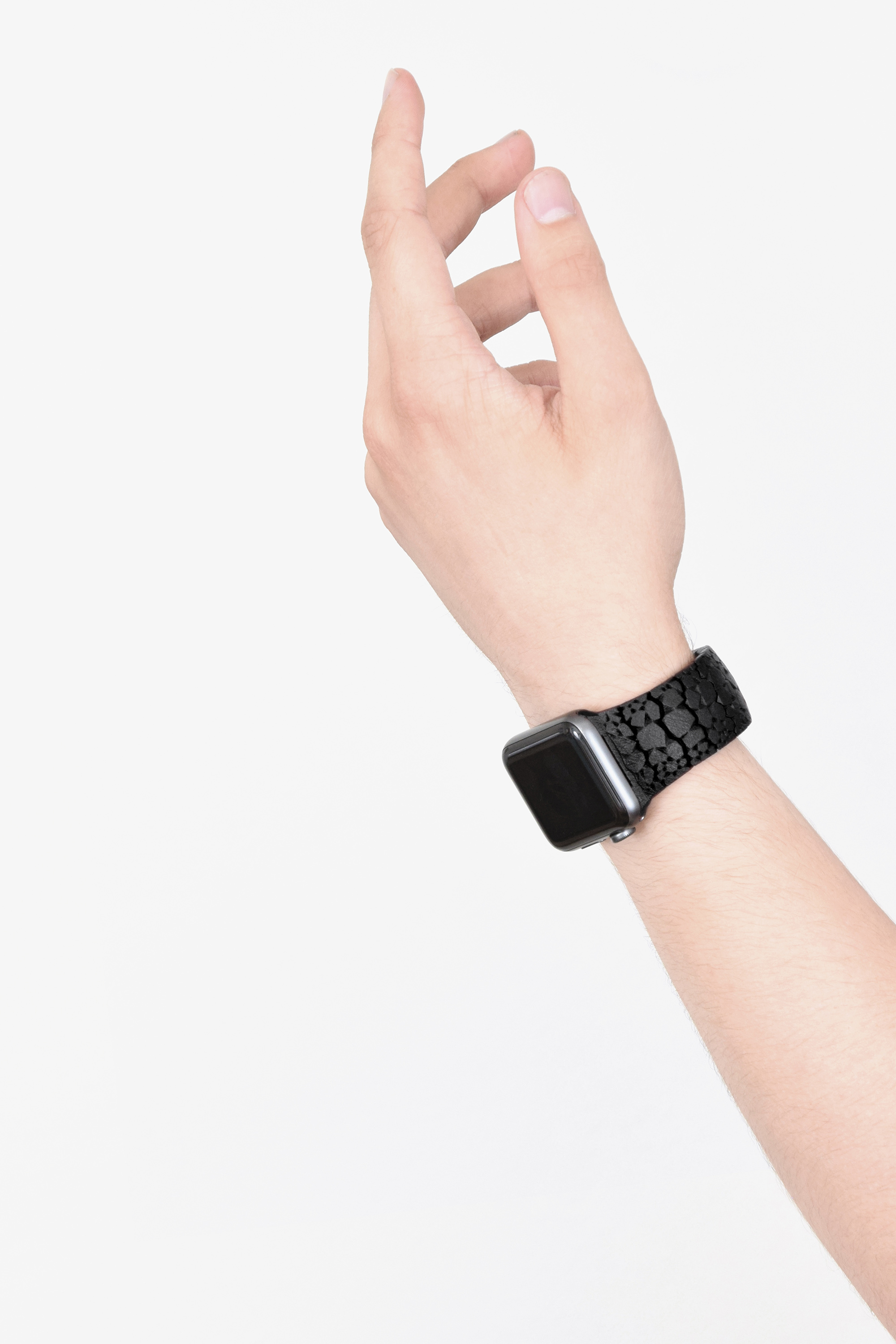
    Apple’s Apple Watch implementation is a shining example of additive manufacturing at scale. Apple now makes two watch cases and a port using additive. Now Bloomberg’s Mark Gurman has stated that,

    “The company’s manufacturing design team along with its operations department is working on ways to 3D-print aluminum, which would bring more efficiency to the production of Apple Watch casings and potentially one day iPhone enclosures.”

    That kind of move by Apple would be sensible if it wants to reduce material usage. Reportedly, this is the goal of the engagement. Summed up, the advantages may include “reduced waste, lower manufacturing costs, improved design flexibility, better structural bonding, and thinner components.” At this current juncture, these goals are, of course, hilarious. Despite adventurous forays into dreamland by current stage suppliers, the economics of Apple’s current 3D printing efforts don’t make sense, right now. But, if we look into a probable future, they may become true and give the company a lasting advantage.

    Far Off Logic

    Apple makes around 40 million watches, over 220 million phones, and over 20 million MacBooks a year. The scale at which the company operates is unsurpassed. At the same time, the firm commands a premium. Not only is Apple selling premium devices, but it also offers a premium experience overall. Committed to excellence and innovation, Apple has to deploy both at scale. This is incredibly difficult to do. Apple is additionally remarkable at how seamless the overall experience is, with objects looking exactly how they feel, for example, and feeling exactly as the tactile response to them. Design at Apple is not skin deep, and the firm has pioneered a total design that is difficult to replicate. With revenues of $416 billion in 2025, Apple dwarfs not only other firms but many sectors and whole economies. So Apple is difficult to compare to other companies; it’s a bit like comparing a galaxy to a planet. So Apple’s logic is not the same as the logic that makes sense for other firms, even very large ones with which it directly competes.

    For Apple to industrialize 3D printing across several metals for handset and wearable production was not an easy decision. At the same time, when Apple industrializes a new material, process, or device, it is the production system that makes the parts (and costs) add up. Apple can’t really place an order at a contract manufacturer or just turn on some machines. Its scale needs to be replicated; there are multiple vendors, and there is an interplay of systems. At the same time, for any effort to make sense, the firm can’t just introduce a new color for a new color’s sake, but rather it needs to make meaningful change happen in its supply chain in order to derive lasting advantage from this change. Pursuant to the effort at the scale and precision that the company demands, changes must be meaningful.

    In the long run, reducing material use is a lasting change that can give the company a lasting advantage. Apple will be able to use metals that others cannot because of cost. This will make Apple products feel more premium while lasting longer. If someone tries to best them in using metals, Apple will have a better-feeling part, which simultaneously would have less material in it. This, in and of itself, explains the firm’s attraction to aluminum. Aluminum’s ubiquity, familiarity, and high production costs, but high reusability make it an ideal material. If Apple can sufficiently elevate this material, it could produce a better experience at comparably lower cost. If it masters this material, then it can make better devices overall. If its production system investment further optimizes its use, then it will reap economies of scale.

    Thinner

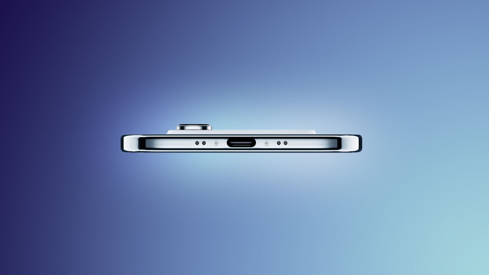
    iPhone Air 3D printed USB-C feature. Image courtesy of Apple.

    Hand in glove with this is the idea of thinner components, which could add up to additional weight savings. Thinner components make for lighter devices that use less material. But, especially in the crowded space of a phone or anything with an antenna, really, more antenna and battery space lead to better devices. With battery life and connectivity being of paramount importance to consumers, thinner other components mean more space for Apple to cram in more functionality. At the same time, by integrating functionality, Apple will reap greater rewards from components made with additive manufacturing. On top of this, making these components conformal or fit into very specific spaces will also bring more benefits to the firm. This can cumulatively add up to huge savings and durable advantages for Apple.

    What’s more, Apple could apply IP to making certain components thinner that could let it gain an advantage over rivals. It could patent certain geometries that would be the most compact battery shape, or the most accordion-like USB-C plug, or the best way to shape a sensor. This would be an IP advantage that the firm could not get with CNC, for example. Thinner is also interesting in that, if it could use metal more efficiently and make devices thinner, it could make it harder for competitors to match devices that contain more polymers.

    Bonding

    One of the advantages of “better structural bonding,” an article explains, is that different textures “create textured internal surfaces that improve bonding between plastic and metal around the antenna housing.” Better bonding is nice, and it may add up to benefits for users and longevity. But if Apple could just change a texture and then use a few drops less of glue or solder, the cost savings would be immense. To me, the material savings are more compelling. But, additionally, there are more things to consider here. Imagine if we could reduce a few soldering or assembly steps by making things easier to join together. Or imagine if we could include a texture that would let a screen drop into place more securely, saving a second on an assembly step? Or could we add a texture that would reduce error rates when placing said screens? Now that would be a huge cost and time saving for Foxconn and Apple. Again, at Apple scale, something like better textures can have profound advantages. To me, however, cycle time and material savings will be meaningful here.

    Improved Flexibility

    So when we look at the idea of “improved design flexibility,” it is not exactly like the geometric flexibility or design freedom that we normally associate with additive. In an Apple context, the big win here is not simply the ability to make a “better” design. What this creates is the ability to optimize overall performance in the cramped interior and, at the same time, create areas of outperformance within the total production system. And we may be able to create a better device. More freedom to create a new shape for an antenna may therefore not only improve the reception of a phone model’s Wifi but also could free up more space for further battery life, translating into lower battery acquisition costs and more margin while allowing for the reduction of several hundred million fasteners because we eliminated one through the new design, which will make the phone thinner. For an Additive application to make sense, we often look for cumulative advantages. In this sense, the total production system that Apple will deploy will reap rewards from multiple effects through seemingly infinitesimal improvements. Combine this with the firm’s waste reduction strategy, and we can see this in the light of remaining competitive at scale.

    Lower Costs

    Now, of course, the lower costs thing is hilarious, especially given the high scrap rates we’re currently seeing. But let’s do a thought experiment. What could Apple do to cost out the process? How would it work?

    If we stick to LPBF, we can see that the case part is problematic, with support needing to be removed and walls and some features being in peril at the time of build plate removal and later. Ports, slots, and the like will continue to be problematic, and we can see why the company has worked hard to eliminate these from its designs. Yes, it’s silly to buy a $900 laptop with one USB port, but it saves a few hundred millionths of an operation. So fewer holes would be nice. Thinner walls would be especially desirable, as they could deliver a better buy-to-fly ratio. At the same time, the case or internal components could become heatsinks, “fasteners,” or be further optimized.

    But if we look at the sheer volume of cases for ports, plugs, speakers, rare-earth magnets, and fasteners, we can see that we could be freeing up a lot of internal real estate. And we could do this with lower-cost components that have big impacts. Again, binder jet or MIM would be the way to go here, but Apple seems to love lasers more than Scan Lab, so who knows. The quicker, easier, and more fundamental win would be to optimize these components over the case, in my opinion. Imagine just removing two screws through an optimized assembly so that the screw fits onto a lower layer! I’d focus on this before working more on larger cases for phones, since the win could be easier and lead to a bigger performance improvement. Also, then maybe I can make a smaller phone?

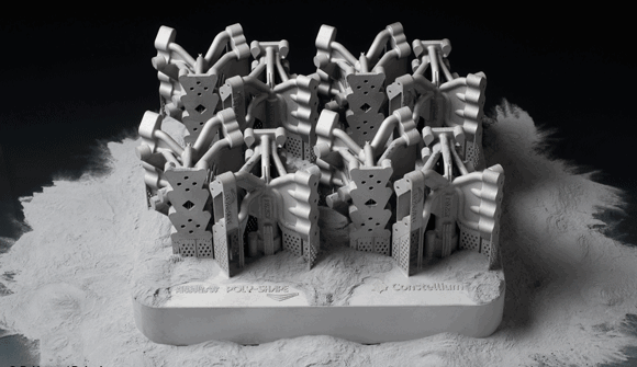
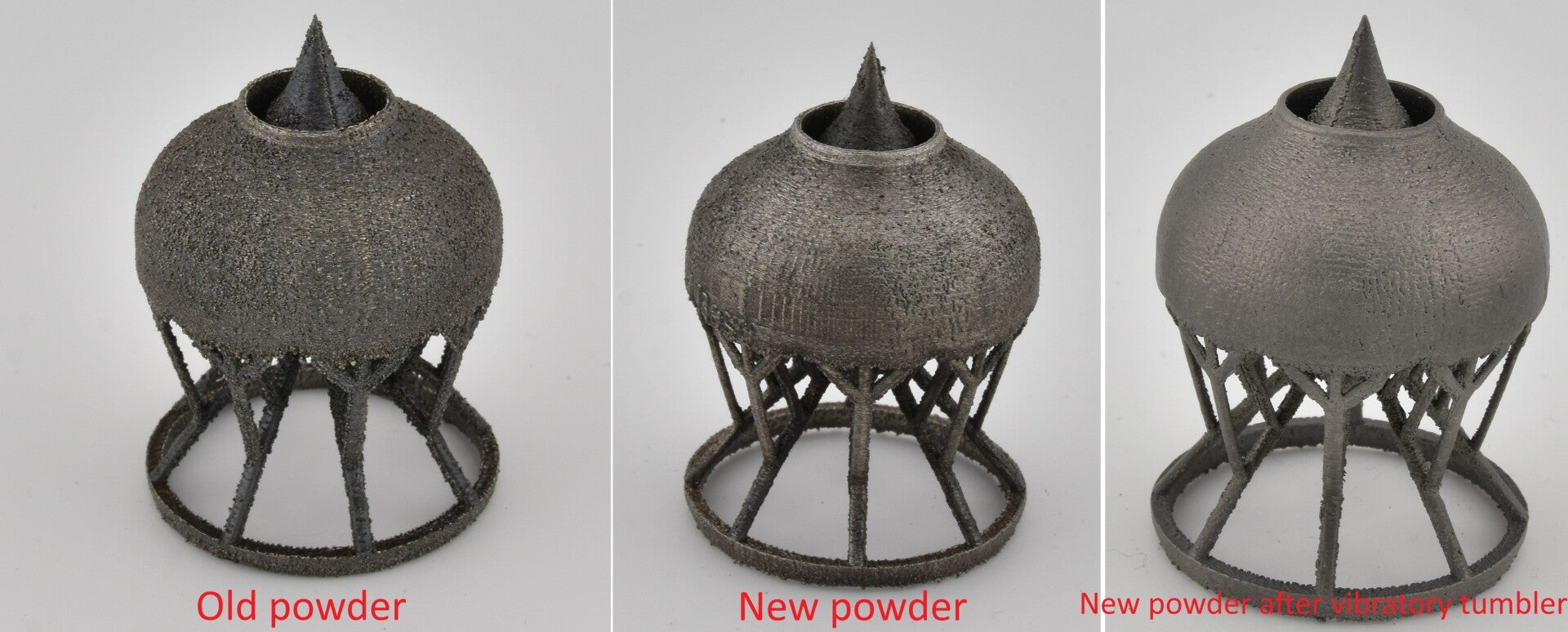
    Constellium’s Aheadd CP1 aluminium powder. Image courtesy of Constellium.

    Assuming that we’d then take this to another level and then tackle phone cases, we’d be dealing with a huge increase in build times, part volume, number of parts, object size, and post-processing time. And risk, risk too. Failure too. Let’s ignore for a second that we would need 2,400 machines. Breathe, let’s talk about the volume, talking 146mm by 72mm to 166mm by 76mm. Depending on the metric, the phone case is three to four times bigger than the watch case. Binder jet would be more limited here; weirdly, e-beam may make more sense than LPBF, given you could pack better and may have less support removal and residual stress. Of course, ebeam sucks for aluminum, so we’d assume that LPBF would win. Personally, I’d use bound filament material extrusion and then mill the ever-living everything out of it for a while. But maybe we want it to have a thin wall thickness and for the case to be a heatsink with hollow parts? Maybe we can make some recessed 3D printed buttons and mount them on some walls to snap the Taptic Engine and other parts into place? There are over 100 fasteners in the latest iPhones. Eliminating some of these through dovetails and other smart ways to slide things into snap-fit elements on the 3D printed case could maybe work?

    Let’s assume we’d do everything with three vendors, each replicating each other’s efforts. We would need completely automated part removal, depowdering, distressing, hipping, all that jazz, including automated build plate resurfacing, CNC milling, and laser marking for recesses/ports. We’d need automated filling with an Azo or similar system and a quite automated build removal process. This is straight out of some German mid-2010 Industrie 4.0 fever dream and seems well within the bounds of what Apple could do and what key suppliers could do. Had they had a laser-based QA system at every major step, maybe to save time? Glidewell implemented a Micro-CT scanning workflow for itself so that Apple could do this too. Just given the turnings Apple already produces and the amount of support and scrap that will be created, even if they are efficient, I’d get a couple of Eigas. Or maybe a Metalworks or two? If they could use residual heat from the factory or some kind of efficient power source to locally make and recycle powder, they could have some interesting gains.

    If I was them I would have bought Incodema3D and told them about a world beyond Inconel, then I’d buy Metal Powder Works for my turnings, a system to recycle aluminum generally into smaller components, Metalysis to make powder more efficiently than anyone else, some kind of solar/waste energy system to power it and made my own Aheadd CP1 kind of thing to save on heat treatment steps. I’d focus on something that could anodize really nicely, so I can give my phones some nice colors quickly. Then they’d need a pulsed-current anodizing process that provides a superior surface finish while anodizing more quickly. Ideally, I could do all of this to achieve thinner wall thicknesses. I’d engineer an aluminum that fits my process, my goals, and the process steps I can eliminate. I’d probably develop my own alloy, what the hell, I’m Apple.

    Alternatively, I’d develop an LPBF machine that could run on MIM powder. Or I’d come up with a process that uses HIP powder in a kind of new-fangled powdered-metallurgy way, letting me make more delicate shapes. Generally, I’d turn to green or blue lasers over regular old fiber. Green lasers would really speed up build times, and this would also go far in explaining why it’s so hard to get powerful green lasers that work well now. On the whole, a standard machine could suffice, but one thing that Apple would really want was paths to create thinner walls and features than are usually possible.

    Now Apple has an interesting patent, this is a kind of dual case comprising two metal materials, one perhaps being preformed and the other an additive part that has a lot of the features that we described above, including “preformed recesses” and also some interesting things like, “micro-features on the scale of 10’s of microns or less to form hydrophobic surfaces, surfaces that feel like glass, or other surface micro-features that promote chemical etching of the surface.” Other parts of the patent talk about adding electrical components or building the part within the volume. Helpfully, I found the patent after writing this article, but you can see that there are different roads, all leading to Rome.

    Unexpectedly, perhaps we can conclude that whereas Apple’s initial foray into 3D printing has not been economically viable (for its suppliers mainly), a further path deeper into 3D printing does make a lot of sense. Also, if we look at the challenges to be overcome here, there is a lot of hard work, engineering, automation, and process control. But there’s no magic leap needed in physics or technology. Apple could do this with current-stage technology optimized for this purpose. And it could, at Apple’s scale, make sense for the company to do so.

  • MIT’s Enterprise Additive Manufacturing Program Heads to RAPID + TCT 2026

    MIT will offer the class Enterprise Additive Manufacturing over the course of five days. Three and a half days will take place at MIT, while two half days will see the students bounce between MIT and RAPID + TCT. The focus is on teaching business leaders how to implement additive at scale and “identify, evaluate, and deploy innovative applications of AM are essential to greater and more effective adoption.” The course covers “strategy, operations, technology selection, and real-world case studies” and will take place in Boston between April 13 and 17.
    The curriculum will cover both the direct manufacturing of 3D printed components and things such as jigs and fixtures. The team believes that “the frontiers of AM are defined by new materials, advanced automation and software, and the use of artificial intelligence for design optimization and production control.” The team at MIT says it has taught 3D printing classes to over 10,000 students to date. Which is actually amazing if you think of it.
    The teams will look at how to assess whether 3D printing could meet their needs while also evaluating it against conventional manufacturing technologies. Cost, volume, and performance will be judged. Not only the additive step, but also design and post-processing will be looked at. Participants will also get to see and work with 3D printers at MIT and get to work with CAD and other 3D printing software.
    Through lectures and discussions, teams of students will learn and apply their knowledge to business cases. Teams will create a vision, business case, design, and strategy. In so doing, they’ll learn how to implement and apply additive to their own business lives. They say that, “We hope you arrive at MIT with an open mind, and leave the course with a clear idea of how to use AM and, more importantly, practical experience in doing so.” The course will be presented through the lens of an actual 3D printed part. Through the business case, design, and costing, they will learn which processes (or if at all), this part will work. At RAPID, the students will see and interact with the parts, machines, technologies, and suppliers they may need for their business case. Teams will be led across the show floor to meet people and see parts. Around 40% of the course will be lectures and 40% will be working in groups. They estimate that 40% of the course will cover additive manufacturing as a technology, 30% will focus on the latest developments, and 30% will cover applying the technology.
    You could be new to 3D printing or have some experience. Engineers, design engineers, managers, doctors, and more have done similar classes at MIT. The team thinks that the sectors “aerospace and defense, medical devices, thermo-electrical components, automotive, fluid handling devices, semiconductors, art, design and architecture, consumer products, and other general manufacturing of physical goods” are the most relevant.
    I really like the work that MIT is doing in educating a broad swathe of interested people. The path towards understanding has traditionally been difficult and long. By making it easier for people to get their bearings, they’re accelerating industry adoption. For over 15 years, I’ve given tours of 3D printing trade shows to investors, business partners, and prospective clients. It’s so much more efficient to show them the machines and parts in person. Showing people the limitations in size, smoothness, materials, and finishes is much faster. Seeing the machines and the build volumes, but also all of the post-processing equipment, really helps people understand where we are. It’s one thing to describe a part, but to hold it and understand is much better. I really think that this kind of thing is very valuable, and I hope we see many more courses include trade show experiences in the future.
  • Singapore 3D Prints Childcare Center Walls in Two Days

    The exterior walls of a childcare center were 3D printed in two days in Singapore. The first story was made with additive while the second was made with conventional methods. This comes amid a push by Singapore to increase the number of early child care places available and to use 3D printed construction. The building is a part of a 348-apartment condominium project in Singapore’s northern Woodlands neighborhood. Woodlands is home to the excellent Marsiling Mall Hawker Centre, known for Ye Lai Xiang Laksa, the excellent Yan Ji Seafood soup, and nearby Nur’s Malay Food. Woodlands is residential, a high-rise kind of place replete with Housing and Development Board (HDB) apartments and their recognizable boxy style. With mangrove, a pair of parks, and sandwiched between Malaysia, a wetland, and the Zoo, it’s a nice place. There’s an Uniqlo, you’re very close to the cheap things and good food of Malaysia, but for Singapore, the place is relatively remote.

    The structure was 3D printed by construction firm Woh Hup. Won Hup isn’t just any construction firm; started in 1927, it is one of the largest local firms and has worked on some of the most iconic and challenging local projects, such as Jewel Changi Airport, the Expo center, and the Gardens by the Bay. The company is now working on around 20 projects across Singapore, including a 63-story residential building, and another twin 62-story residential building with a third 36-story building next to it. Won Hup builds subway stations, golf courses, giant malls, and government buildings. The scope for additive is therefore considerable. As well as Won Hup, the National University of Singapore (NUS), the Building and Construction Authority (BCA), and the National Additive Manufacturing Innovation Cluster (NAMIC) worked on the project.

    The Straits Times quoted Du Hongjian of the NUS College of Design and Engineering saying that,

    “(It) needs to be set up one day before casting, and can only be removed one to two days after concrete is cast. 3D concrete printing can reduce the amount of manpower involved, and offer a higher degree of design freedom for architects and structural consultants.”

    He also stated that it is cheaper than formwork, the Straits Times said: “The walls on the first level of the centre were printed in two days, and required a team of around six construction workers tasked with responsibilities such as monitoring the sensors that track the quality of the concrete mixed on-site. Three additional checkers were also deployed to ensure that the novel process went smoothly. The work took a total of 170 manhours, whereas manual building would have required nearly 400 manhours and a larger team of 11.”

    Now used as a structural element, concrete is advancing in Singapore. Compression, load-bearing, bending, and shear-bending were tested on the structure. One thing that was pointed out is that construction could take place later in the evening, resulting in less noise pollution, a benefit that I had not previously heard about. The 3D printed concrete also needed more cement and therefore a higher emissions overall concrete mix than regular concrete. Still, the team is trying to resolve this by using 60% glass powder in the mix. The Co2 emissions would be reduced by half, and their calculations show that it would retain the same strength.

    The higher Co2 emissions are something that needs to be talked about more by the 3D printed concrete community. Just saying that it is more sustainable because it uses less material is not enough. And using glass powder in this way, readily available globally, could be a great boon to the 3D printing construction industry.